Spectroscopy systems and solutions provider Horiba Scientific (Piscataway, NJ) has partnered with Covalent Metrology (Sunnyvale, CA), a provider of analytical services, to expand engineering and scientific access to expertise and chemical analysis instruments.
An important part of the partnership is the opening of the Horiba Scientific North American Demonstration Lab at Covalent’s Sunnyvale headquarters. This showroom is Horiba’s first demonstration lab with a partner in North America and joins its application/demo labs in its corporate offices. It will showcase the company’s spectroscopy solutions, as well as bolster the companies’ mutual efforts to develop methods for new chemical analysis applications. With access to Horiba’s instruments, Covalent’s team of experts will be better able to support clients with more accurate and powerful chemical analysis capabilities.
In addition to applications development, the demonstration lab will position both companies to accelerate research and development work in the semiconductor, electronics, and advanced materials industries throughout the North American region.
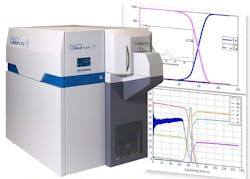
The inaugural instrument installed in the Horiba showroom is the Horiba GD-Profiler 2 system for glow discharge optical emission spectroscopy (GDOES). The tool is designed for high-speed, quantitative analysis of all elements of interest, including nitrogen, oxygen, hydrogen, and chlorine. It is an ideal tool for thin and thick films characterization and process studies. It also captures direct measurement of depth (with nanometric precision) simultaneously with element quantification to achieve maximum efficiency and accuracy for depth profiling on layered materials and multiphase samples. Analytical services requiring GDOES are available now for customer work.
