TOM POMPOSO
The confocal laser scanning microscope has evolved into a tool with very high resolution capabilities. The recent inclusion of a violet-emitting diode laser as the illumination source has accelerated this evolution. Just as the semiconductor industry has shifted to light sources with shorter wavelengths to produce smaller feature sizes, the microscopy industry has also moved toward the blue. In fact, the microscopy industry must use shorter-wavelength sources so it can image and measure the smaller features being produced by the semiconductor industry.
The blue-violet confocal system has pushed the optical resolution barrier down into the domain traditionally occupied by scanning electron microscopes (SEMs). Attached to a standard optical microscope, a short-wavelength confocal system produces SEM-level resolution without the vacuum or gold coating necessary for SEM imaging. The system can also measure height and depth, as well as profile a surface.
Optical layout
Light from a 410-nm diode laser is passed through a beam expander and an acousto-optic device that scans the beam horizontally at a standard 15.73-kHz TV rate. The beam then strikes a galvanometer-driven mirror, providing vertical deflection. After passing through a quarter-wave plate, the beam is focused by an objective lens onto the specimen surface, which it scans in a raster pattern. The reflected light returns along the same optical path and is diverted by a beamsplitter to a 1000-element linear CCD matching the direction of the horizontal scan.
The scan across the sample is a standard TV raster, with the vertical scan a 525-sequential-line scan per frame. The light reflected from the sample is directed onto the CCD element. Because the CCD is a linear device, the horizontal line scan on the CCD is a repeated scan, while the scan on the sample is sequentially scanned. The output of the CCD is fed to the Z input of a video monitor, which displays the image for individual or group viewing. The image is a real-time image, allowing the sample to be viewed while being repositioned. If the sample is a dynamic sample and is changing shape or otherwise moving, it can be videotaped at standard National Television Standards Committee rates.
An appropriate aperture removes defocused light rays. Only focused confocal slices are displayed on the monitor. The aperture allows only the center, high intensity portion of the laser beam to be used, which provides an additional decrease in spot size and increased resolution. The outer circumference of the laser beam is blocked by apertures at appropriate positions in the optical path.
Imaging at SEM magnification
Because the horizontal and vertical deflection distance of the laser is constant, optical magnification is changed by rotating a different objective lens into place. Magnifications from 370X to 15,000X can be displayed on the video monitor. The magnification can also be changed electronically by using a smaller portion of the CCD. Three-dimensional (3-D) images can be displayed up to 50,000X, with a resolution of 40 nm equivalent to that obtained from SEMs.
A DC drive motor, which is stepped in 50-Å increments, drives the focus of the optical microscope. This stepping process is used to generate confocal slices that are collected to create an image that has three-dimensional (3-D) information. This image can be used to measure between points in 3-D space or to create a 3-D image.
The applications for this type of tool are many. Any type of sample, including a liquid, can be rapidly imaged without time-consuming sample preparation. Semiconductor and optical devices such as Bragg diffraction gratings and optical filters, which normally collect charge under an electron beam, can be easily imaged at high magnification. Even the meniscus of a liquid in a container and drops of liquid on a glass slide have been successfully imaged and profiled with this instrument.
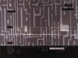
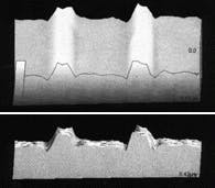
A semiconductor photoresist pattern can be imaged at 5600X magnification (see Fig. 1). Further magnification of another photoresist image to 50,000X shows 3-D image information (see Fig. 2).Samples viewed as is
Samples do not have to be specially treated in any way. Images can be obtained quickly, without gold coating or evacuation, by simply placing the samples on a standard optical microscope stage for image acquisition. In addition to use at high resolution, the blue-violet confocal microscope has many applications at lower resolution, including measurements and imaging of subsurface microcracks or defects in glass materials used for fiberoptic components. Waveguide structures and ceramic materials, which are virtually impossible to image optically, can easily be imaged with confocal instrumentation and structure heights and widths rapidly measured. Defects on the surface—or beneath the surface, if the material is transparent—can easily be identified.
The instrument has also been used with optical microscopes that use long-working-distance lenses, turning low-resolution results normally obtained from these low-numerical-aperture lenses into the equivalent of results obtained from high-numerical-aperture lenses.
Other uses are many and varied. Metals can be measured in their molten state, with their phase changes imaged in real time and captured on videotape. A portable version of the confocal laser microscope—in which the microscope is placed on the sample and the objective lens scanned to collect confocal slices—can image and measure the surface roughness of chemical-mechanical polishing pads and 500-µm-deep wear grooves on the pads. This portable version has also been used to measure the depth of microcracks in the steel-walled furnace of a gas fired boiler. The portable head was held firmly to the wall in a vertical position, and depth and width measurements were taken of cracks in the steel wall.
Tom Pomposo is director of sales for Lasertec USA Inc., 1778 Technology Drive, San Jose, CA 95110; e-mail: [email protected].

